This is part of a series of posts analysing the Chip-8 interpreter on the RCA COSMAC VIP computer. These posts may be useful if you are building a Chip-8 interpreter on another platform or if you have an interest in the operation of the COSMAC VIP. For other posts in the series refer to the index or instruction index.
INSTRUCTION GROUP: 7XNN
Add NN to VX
INSTRUCTION GROUP: 8XY1
OR VY with VX
INSTRUCTION GROUP: 8XY2
AND VY with VX
INSTRUCTION GROUP: 8XY3
XOR VY with VX
INSTRUCTION GROUP: 8XY4
Add VY to VX, load VF with carry bit
INSTRUCTION GROUP: 8XY5
Subtract VY from VX, load VF with carry bit
INSTRUCTION GROUP: 8XY6
Shift VY one bit right, load VX with result, load VF with bit 0
INSTRUCTION GROUP: 8XY7
Subtract VX from VY, load VX with result
INSTRUCTION GROUP: 8XYE
Shift VY one bit left, load VX with result, load VF with bit 7
The first of these instruction groups, 7XNN, adds the immediate operand NN to VX. It’s simple enough to not warrant a flowchart, so here’s the code:
Labels | Assembly | Comments |
7XNN: | 45 | Get the value in the second byte of the instruction into the accumulator (D) and then advance the Chip-8 programme counter to the next instruction. |
01B8 | E6 | Set the VX pointer to be used for register indirect addressing instructions. |
01B9 | F4 | Add the value in VX to the accumulator (D), which currently holds the immediate operand from the second byte of the Chip-8 instruction |
01BA | 56 | Store the result back in VX. |
01BB | D4 | Return to the fetch and decode routine |
An important thing to note about this routine is that any carry is ignored. If the result is more than 0xFF then only the least significant byte will be stored. For example, if V0 is 0xF1 and the instruction is 7010 then adding 0x10 to 0xF1 should give 0x101. However, since only the least significant byte will be preserved, VX will contain 0x01 after this operation. Because the carry bit is not preserved, subsequent arithmetic operations on the value in VX would be inaccurate. If you need addition that preserves the carry bit, use instruction group 8XY4 instead (see below).
This instruction requires 10 machine cycles (45.4 microseconds).
The instruction groups that begin 8X?? all work in the same way, using a single routine. They make use of the fact that there is a series of 1802 instructions (0xF1 to 0xF7 and 0xF9 to 0xFF) that perform arithmetic and logic instructions. Instructions 0xF9, 0xFA, 0xFB, 0xFC, 0XFD and 0xFF all use immediate operands, so they cannot be used. The remaining instructions 0xF1, 0xF2, 0xF3, 0xF4, 0xF5, 0xF6, 0xF7 and 0xFE all operate on either the accumulator alone or the accumulator and whatever memory location is currently pointed to by the register indicated by X, so these instructions can be made use of by the Chip-8 interpreter. The flowchart shows how the routine works:
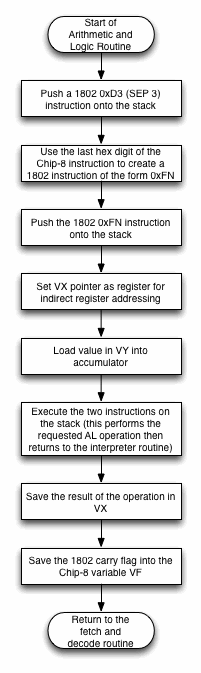
Here’s the code:
Labels | Code (hex) | Comments |
8XYN: | AF | Get the value in the second byte of the instruction into the accumulator (D) and then advance the Chip-8 programme counter to the next instruction. |
01BD | FA 0F | Mask the byte to save just the second hex digit. |
01BF | 3A C4 | If the second digit is not zero, it’s an arithmetic and logic instruction, so branch to the decode routine for these. |
01C1 – 01C3 | There’s a short routine here to copy VY into VX. This was analysed in a previous post. | |
DECODE_ AL_ INSTR: | AF | Temporarily save the last digit of the instruction in RF.0. |
01C5 | 22 | Decrement the stack pointer, ready for a push operation. |
01C6 | F8 D3 | Load a 0xD3 1802 instruction (SEP 3) into the accumulator. |
01C8 | 73 | Push this onto the stack and decrement the stack pointer. |
01C9 | 8F | Restore the last digit of the Chip-8 instruction to the accumulator. |
01CA | F9 F0 | OR this with 0xF0 to create a 1802 instruction of the form 0xFN, where N is the last hex digit of the Chip-8 instruction. |
01CC | 52 | Push this onto the stack. |
01CD | E6 | Set the VX pointer to be used for register indirect addressing memory instructions. |
01CE | 07 | Load the value in VY into the accumulator. |
01CF | D2 | Execute the two instructions at the top of the stack (the first of these will be the AL instruction, the second will be a SEP 3 instruction to return control to this routine at the instruction following this one. |
01D0 | 56 | Save the result of the operation in VX. |
01D1 | F8 FF | 0xFF is the low-order byte of the address of Chip-8 variable VF. |
01D3 | A6 | The VX pointer now points to VF. |
01D4 | F8 00 | Clear the accumulator. |
01D6 | 7E | Move the carry flag into the least significant bit of the accumulator. |
01D7 | 56 | Save this in VF. |
01D8 | D4 | Return to the fetch and decode routine. |
There are a few interesting things to note about this routine. Firstly it cleverly uses the stack as a temporary scratch pad for a dynamically created, two-instruction routine that performs the actual arithmetic or logic instruction. You might have noticed that although two instructions are pushed onto the stack at the start of the routine, they are never popped off again. This is because, when the routine is run, R2 (the stack pointer) is incremented after each instruction is executed. So when control is returned to the Chip-8 interpreter routine, R2 has been restored to its original position.
Note that all these instructions overwrite variable VF. This is used to show the status of the carry bit, which is copied into the least significant bit of VF. All other bits of VF will be set to 0. This means, if you use VF as the VX argument, the result will be overwritten by the flag status.
Only the first five of these instructions were officially documented by RCA. 8XY6, 8XY7 and 8XYE are all undocumented. Unfortunately an erroneous assumption about 8XY6 and 8XYE, the two shift instructions, seems to have crept into Chip-8 lore at some point. Most recent documentation on Chip-8 suggests these instructions shift VX rather than VY. Some documents suggest that the correct format for them is 8X06 and 8X0E. However, when these instructions are run on the original Chip-8 interpreter, they will shift VY not VX! An instruction of the form 8X06 or 8X0E will not work as expected. The programmer would be expecting this to shift VX and store the result back in VX. What would actually happen is that V0 would be shifted and the result stored back in VX. This leaves the programmer of a contemporary interpreter with a bit of a dilemma. Do you make these instructions function as they would have done in the original interpreter or do you make them function in accordance with the erroneous assumption? Or do you offer both modes and a way to switch between them? This post documents the way the instructions worked in the original Chip-8 interpreter.
All these instructions require 44 machine cycles (199.76 microseconds) to execute.
The table below shows the register state for VX, VY and VF for each of these instructions.
Instruction | VX (entry) | VY (entry) | VX (exit) | VY (exit) | VF (exit) |
8XY1 | VX argument | VY argument | Bitwise OR of VX with VY | Unchanged | Undefined |
8XY2 | VX argument | VY argument | Bitwise AND of VX with VY | Unchanged | Undefined |
8XY3 | VX argument | VY argument | Bitwise XOR of VX with VY | Unchanged | Undefined |
8XY4 | VX argument | VY argument | VX added to VY | Unchanged | 0x00 if no carry occurred, 0x01 if a carry occurred |
8XY5 | VX argument | VY argument | VY subtracted from VX | Unchanged | 0x00 if a borrow occurred, 0x01 if no borrow occurred |
8XY6 | VX argument (initial value is irrelevant) | VY argument | VY shifted right by one bit. Most significant bit of VX will be set to 0 | VY shifted right by one bit. Most significant bit of VY will be set to 0 | 0x00 if least significant bit of VY before shift was 0, 0x01 if least significant bit of VY before shift was 1 |
8XY7 | VX argument | VY argument | VX subtracted from VY | Unchanged | 0x00 if a borrow occurred, 0x01 if no borrow occurred |
8XYE | VX argument (initial value is irrelevant) | VY argument | VY shifted left by one bit. Least significant bit of VX will be set to 0 | VY shifted left by one bit. Least significant bit of VY will be set to 0 | 0x00 if most significant bit of VY before shift was 0, 0x01 if most significant bit of VY before shift was 1 |
Note that when VF is shown as undefined, VF will still have been set to either 0x00 or 0x01, but this will reflect whatever 1802 instruction last affected the DF register and will bear no relation to the outcome of the current instruction.
Another thing to note is that, although some of these instructions set VF to reflect whether a carry or borrow occurred or to reflect the bit that was lost in a shift operation, none of these instructions take that status of VF into account when they are executed. This means the programmer must explicitly take whatever action is necessary as a result of the value in VF. For example, if the programmer was adding two four-byte integers, they would have to check VF after each addition operation and, if necessary, manually increment one of the addends for the next addition operation before performing it.
Here are examples of each instruction:
8XY1 (VX OR VY)
VX (entry): 0x00101101 (0x2D)
VY (entry): 0x01001011 (0x4B)
VX (exit): 0x01101111 (0x6F)
8XY2 (VX AND VY)
VX (entry): 0x00101101 (0x2D)
VY (entry): 0x01001011 (0x4B)
VX (exit): 0x00001001 (0x09)
8XY3 (VX XOR VY)
VX (entry): 0x00101101 (0x2D)
VY (entry): 0x01001011 (0x4B)
VX (exit): 0x01100110 (0x66)
8XY4 (VX + VY resulting in no carry)
VX (entry): 0x00101101 (0x2D)
VY (entry): 0x01001011 (0x4B)
VX (exit): 0x01111000 (0x78)
VF (exit): 0x00000000 (0x00)
8XY4 (VX + VY resulting in carry)
VX (entry): 0x11101101 (0xED)
VY (entry): 0x01001011 (0x4B)
VX (exit): 0x00111000 (0x38)
VF (exit): 0x00000001 (0x01)
8XY5 (VX – VY resulting in no borrow)
VX (entry): 0x01001011 (0x4B)
VY (entry): 0x00101101 (0x2D)
VX (exit): 0x00011110 (0x1E)
VF (exit): 0x00000001 (0x01)
8XY5 (VX – VY resulting in borrow)
VX (entry): 0x00101101 (0x2D)
VY (entry): 0x01001011 (0x4B)
VX (exit): 0x11100010 (0xE2)
VF (exit): 0x00000000 (0x00)
8XY6 (SHR VY with 0 as LSB)
VY (entry): 0x00101100 (0x2C)
VX (exit): 0x00010110 (0x16)
VF (exit): 0x00000000 (0x00)
8XY6 (SHR VY with 1 as LSB)
VY (entry): 0x00101101 (0x2D)
VX (exit): 0x00010110 (0x16)
VF (exit): 0x00000001 (0x01)
8XY7 (VY – VX resulting in no borrow)
VX (entry): 0x00101101 (0x2D)
VY (entry): 0x01001011 (0x4B)
VX (exit): 0x00011110 (0x1E)
VF (exit): 0x00000001 (0x01)
8XY7 (VY – VX resulting in borrow)
VX (entry): 0x01001011 (0x4B)
VY (entry): 0x00101101 (0x2D)
VX (exit): 0x11100010 (0xE2)
VF (exit): 0x00000000 (0x00)
8XYE (SHL VY with 0 as MSB)
VY (entry): 0x00101101 (0x2D)
VX (exit): 0x01011010 (0x5A)
VF (exit): 0x00000000 (0x00)
8XYE (SHR VY with 1 as MSB)
VY (entry): 0x10101101 (0xAD)
VX (exit): 0x01011010 (0x5A)
VF (exit): 0x00000001 (0x01)
If you are writing an interpreter to strictly mirror the documented functionality of the original Chip-8 interpreter, then you only need to implement instruction groups 7XNN and 8XY1 through 8XY5. However, if you do so, you will almost certainly find some more recent Chip-8 programmes that don’t function correctly.
If you do decide to implement the undocumented instructions, then you need to decide whether to implement the shift instructions as they are shown here (i.e. mirror the behaviour of the original interpreter) or implement them as they are documented by most recent descriptions of the Chip-8 instruction set (i.e. with VX being shifted rather than VY). Alternatively, you could provide both behaviours and then allow users to switch between them if they need to. The reality is that you will probably find more Chip-8 programmes that depend on the erroneous behaviour, so that may be a better choice as a default.
Be First to Comment