In an earlier post on Chip-8, I mentioned that the RCA 1802 processor has a maximum addressable range of 64K in terms of external memory. Very little of this range is used in the basic COSMAC VIP.
The COSMAC VIP has a 512 byte ROM, which is mapped from 0x8000 to 0x81FF. The base system had 2K of RAM mapped from 0x0000, but this could be expanded to 4K of onboard memory or up to 32K with an external module.
From a reset, the 1802 always begins programme execution from address 0x0000. So, if programme execution starts at 0x0000 and the ROM is located at 0x8000, how does the operating system get executed? That’s a very good question and the answer demonstrates the genius of the system’s designer, Joe Weisbecker.
When the system is first powered up, a latch holds line MA7 on the address bus high whenever the address bus holds the high order byte of the address. This means that, even though the CPU is requesting the byte at address 0x0000, the actual address on the bus will be 0x8000. Effectively the latch is creating a shadow of the ROM from address 0x0000, because a request for the byte at address 0x0000 and 0x8000 will yield the same result, which is to deliver the first byte stored in the ROM. The same latch inhibits selection of the RAM chips so the RAM will not respond to read or write requests.
So you can see that, even though the 1802 is ostensibly executing a programme starting at 0x0000, it is actually executing the operating system held in the ROM at 0x8000. Ok you ask, so that’s how the operating system gets executed, but doesn’t that make the RAM inaccessible? For the moment, yes. So the first task of the operating system is to enable access to the RAM.
Before it can do this, it must first ensure that the CPU is executing the operating system from the physical location above 0x8000 rather than the shadow location at 0x0000. It does this simply by setting one of the registers to point to the correct location in the physical ROM and then designates this register as the program counter. From this point, the operating system is being run at its correct location, but any attempt to address memory from 0x0000 will still result in the ROM being accessed.
The latch that is holding MA7 high when the high order part of the address is on the bus can be set or reset programmatically. It is connected to the IO control lines such that an OUT 4 instruction will reset the latch. The operating system uses this so that, from this point on, RAM will be selected by any address from 0x0000 and ROM will be selected by any address above 0x8000.
Something to note about this design is that, even though the operating system requires a mere 512 bytes, no RAM can be addressed beyond 0x8000. This is why the maximum RAM expansion for the VIP is 32K. As even the base 2K was a generous amount of RAM at the time, this was undoubtedly seen as a workable compromise.
The Chip-8 interpreter is not part of the operating system. It’s a machine language programme that must be loaded to location 0x0000 before it is executed. So if the Chip-8 interpreter resides in the VIP’s RAM, where does the user’s Chip-8 programme go? The answer is that it also sits in RAM, but above the Chip-8 interpreter. The design of the 1802 allows this because the tape system restores data to a specific location in memory. So, the user can load the interpreter and then load a program to another section of the RAM. For convenience, they also have the option of saving both the interpreter and their programme as a single file.
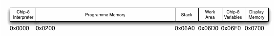
The interpreter occupies the RAM from 0x0000 to 0x01FF, so it expects to find the user’s programme from address 0x0200 onwards. In an interpreter written for a contemporary device, the user’s programme should be loaded at 0x0200 in the virtual machine RAM and the interpreter should begin execution from that point. However, the original Chip-8 interpreter began execution from 0x01FC. The interpreter includes two permanent Chip-8 instructions at this location that are always executed at the start of every programme. The first of these, 0x00E0, clears the display RAM by setting all the bits to zero. The second, 0x004B, calls a machine language routine within the interpreter that switches the VIP’s display on. Anyone implementing an interpreter on a recent device probably doesn’t have to worry about switching the display on, so the only implication of this is that you should ensure the display has all bits set to zero before any Chip-8 programme is run.
Not all the remaining RAM is available to Chip-8 programmes. The final 352 bytes of on-card RAM are reserved for storing Chip-8 variables, the stack and the display memory. So, on a 2K system, you can use the memory from 0x0200 to 0x069F. This 1184 bytes can hold 592 Chip-8 instructions. With a 4K system, you can use the memory from 0x0200 to 0x0E8F. This is 3216 bytes, which will hold 1608 Chip-8 instructions. It is common for modern interpreters to support the 4K configuration.
Now let’s look in more detail at what gets stored in the final 352 bytes of RAM. For this discussion, I’ll show the addresses that would apply in the 2K configuration. For the 4K configuration, simply substitute E or F respectively for the 6 or 7 in the second hex digit of the address.
First up is the stack. This occupies the 48 bytes from 0x06A0 to 0x06CF. This is sufficient to allow 12 levels of nested subroutines. The stack is filled from 0x6CF downwards.
Next is a work area that occupies the space from 0x06D0 to 0x06EF. This is used to assemble sprites ready for writing to the display memory. Chip-8 sprites are one byte (eight pixels) wide, but they have to be assembled across two bytes to allow for the pixel offset, which depends on their x position. As the maximum height for a sprite is 15 pixels, this requires a work area of 30 bytes. The work area is actually 32 bytes so that the variables which follow are stored at addresses in which the least significant digit is the same as the number of the variable.
Chip-8 uses 16 1-byte variables, labelled V0 to VF. These are stored from 0x6F0 to 0x6FF.
Finally we have the display memory, which occupies the whole of the final page of RAM from 0x0700 to 0x07FF. Because Chip-8 has a monochrome display, only one bit is needed for each pixel, which can either be on or off. So each byte of display memory holds eight pixels. The display memory is arranged as 32 rows of 8 bytes, giving a display size of 64 pixels wide by 32 pixels high. I’ll have more to say about the display in a future post.
Here’s a memory map summarising the Chip-8 memory allocation on a 2K COSMAC VIP:
It’s worth noting that Chip-8 programs are not intended to access any of these areas directly, only through the relevant Chip-8 commands. So there is nothing that compels a programmer of a contemporary interpreter to follow this memory allocation scheme. All that is required is that Chip-8 programs are loaded and executed from 0x200 and sufficient memory is made available and can be addressed by the Chip-8 instructions. The stack, the Chip-8 variables and the display memory can be implemented in whatever way the interpreter’s designer sees fit, provided they behave in a way that is consistent with the original Chip-8 interpreter.
And of course, it is unlikely that you will need the space from 0x0000 to 0x01FF that was occupied by the interpreter in the COSMAC VIP. So what then happens to this empty space? The expectation in a modern interpreter is that a set of sprites representing all sixteen hexadecimal characters will be stored there. I’ll be looking at these sprites more closely in a future post.
Be First to Comment